Product Introduction
FCBGA, also known as Flip Chip Ball Grid Array, is an integrated circuit packaging technology that directly flips and installs bare chips onto a substrate. It uses tiny solder balls as electrical connection points to interconnect chips and substrates.
Product Features
High density interconnection: Supports a large number of I/O pins, which are distributed in an array on the entire surface of the bottom of the package, achieving higher pin density than traditional packaging. It can meet the requirements of high-performance computing, communication devices, etc. for high data transmission rate and low latency.
Low inductance and low resistance connection: The distance between the chip and the substrate is close, and the signal transmission path is short, reducing parasitic inductance, resistance and other effects, improving signal integrity and performance, and can withstand higher frequencies, effectively breaking through the overclocking limit.
Better heat dissipation performance: The design of direct contact with the substrate is conducive to rapid heat conduction, and the back of the chip can directly dissipate heat by contacting the air. The heat dissipation ability can also be further strengthened by adding metal layers to the substrate or installing metal heat sinks, improving the stability of the chip during high-speed operation.
Miniaturization: Compared with traditional wire bonding packaging, FCBGA can significantly reduce the packaging size, making it suitable for applications with strict space requirements, such as mobile devices, wearable devices, etc.
application
FCBGA packaging can meet the high data processing and transmission requirements in fields such as CPU, GPU, 5G base station, optical communication module, smart home, medical equipment, industrial control, and the Internet of Things.
process characteristics
Unique chip connection method
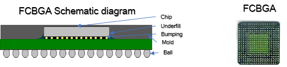
Using flip chip technology, the metal contacts of the chip are directly connected to the solder ball pads on the packaging substrate. The interconnection between the die and the carrier is achieved through conductive “bumps” directly placed on the surface of the die, and then the chip is flipped and placed face down, with the bumps directly connected to the carrier. This connection method shortens the connection distance between the chip and the substrate, reduces signal transmission delay, and leaves more space below the chip for other functions.
Special packaging substrate
The FCBGA packaging substrate is usually made of Ajinomoto laminated dielectric film (ABF) produced by Ajinomoto in Japan as the laminated insulating dielectric material, and manufactured using the semi additive method (SAP). It has the characteristics of multiple layers, large area, high circuit density, small line width and spacing, and small through-hole and blind hole diameters, which can achieve high-speed and multifunctional LSI chips. However, the processing difficulty is much greater than some other packaging substrates.
Superior electrical performance
Electrical connection is achieved through solder balls, which have low resistance, low inductance, and good signal transmission characteristics. In high-speed signal transmission, it can better maintain the integrity of the signal, reduce signal distortion, improve the accuracy and speed of data transmission, and thus enhance the overall performance of the chip. It is particularly suitable for applications with high electrical performance requirements such as high-speed communication and high-frequency signal processing.
Adapt to multiple types of chips
Suitable for various types of chips, including high-performance chips such as CPUs, microcontrollers, and GPUs, as well as network chips, communication chips, storage chips, digital signal processors (DSPs), sensors, audio processors, etc. Can meet the packaging requirements of different types of chips and maintain stable performance in different working environments.
Substrate Size(mm) 240×76.3
Underfill type: CUF/MUF
Assy Yield 99.9%
Tester:S100、J750、V93K,Handler:CRH8508、HT-1028C
